Logic probes. Simple LED TTL Level Logic Probe
The leads of most elements located on one side of the printed circuit board are bent over the edge of the board and the sub-solders to the contact pads located with reverse side fees. The probe needle is soldered into the groove of the printed circuit board. Capacitor C2 consists of two 10 μF capacitors K53-16 connected in parallel.
In the probe, you can use transistors KT361 and KT373 with any letter indices, possibly usingand other silicon high-frequency transistors of the corresponding type of conductivity. Diodes can be replaced with any low-power silicon ones ( v 3 v 4) and germanium (v 5, v b). microcircuits - similar to other TTL series.
The probe proposed by N. Pastushenko and A. Zhizhchenko (Kiev) allows you to study logical devices in static and dynamic modes.
The schematic diagram of the probe is shown in Fig. 3.
If there is no signal at the input of the element di .1 - low logic level, at the inputs of the elements d 1.2, d1. 3 d1 .4 - high. The indicator segments do not light up. If the input of the probe receives a level corresponding to logical “1”, then the output of the element di.i there will be a logical "O" at the output d 1. 2 - logical “1”, elements d1. 3 and d 1. 4 remain in original condition. The segments light up b and c and the number “1” is displayed. When there is a logical “O” at the input of the probe, then at the output of the elements di .2, d 1.3 and d 1.4 there will be a high logical level and segments a b, c will light up d, e, f.
When applying a probe to the input, itpulses with a frequency of up to 25 Hz, the alternation of the numbers “O” and “1” is visible to the eye. At frequencies above 25 Hz, the influence of capacitor C1 begins to affect. As a result, the brightness of the segment d sharply decreases and the letter “P” is displayed, indicating a sequence of pulses with high frequency at the probe input.
The probe is powered directly from the device under test. If there is +5 V power, segment A (dot) lights up.
The probe uses MLT-0.125 resistors. capacitors K50-6. Instead of a microcircuit k 133La 8 You can use the K155LA8 chip.
In Fig. Figure 4 shows the arrangement of parts on a printed circuit board made of double-sided foil fiberglass, and Fig. 5 - drawings of both sides of the printed circuit board. Appearance the probe is shown in the photograph (Fig. 6)
A probe with a sufficiently large input impedance and high precision response at certain input voltage levels was proposed by V. Piratinsky and S. Shakhnovsky from Moscow.
The transition zone from the state in which the indicator LED is illuminated at full brightness to the state in which the LED is not illuminated is 30 mV for the upper limit of the logical level “0” (-0.4 V) and 80 mV for the lower limit of the logical level “ i" (+2.4 V).
The probe is characterized by low energy consumption from the power source of the device under test, amounting to no more than 12 mA.
In Fig. 7 shows the fundamental electrical diagram sample It consists of two independent threshold circuits, one of which corresponds to level “0”. and the other - level “i”.
When the voltage at the probe input is between 0 and +0.4 V. transistors v 7 and v 8 threshold circuit "1" is closed and the red LED v 5 does not burn. In the threshold circuit "0" transistor v 9 closed and the transistor vi 0 open and green LED is on v 6 . indicating the presence of a logical level “0”.
At a potential at the probe input from +0.4 V to +2.3 V, transistors v 7 and v 8 still closed, transistor v 9 is open and v10 is closed. In this case, both LEDs do not light up. The same thing is observed if there is no signal at the probe input.
No indication, therefore. indicates that. that there is no potential at the input or that it has an intermediate value in relation to the logical levels.
When the voltage at the probe input is above +2.3 V, the transistors open v7, v8 threshold circuit "i"(v 7, v 8 fully open at a potential above +2.4 V) and the red LED lights up v5, indicating the presence of logical level "1". The threshold circuit “0” is in the same state. Diodes vi - v 4 serve to increase the voltage at which the threshold circuit “i” is triggered
Current transfer coefficient h 21eThere must be at least 400 transistors. Diodes vi-v4 KD103 (K102) are unframed. All OMLT resistors are 0.125 - 5%.
The probe is adjusted using a voltage divider connected to a +5 V source, supplying the required voltage level to the probe input.
Changing the value of the resistor resistance r 7 are trying to go outgreen LED v 6 at an input voltage level of 0.4 V, and by changing the resistor resistance r 5 - red LED lights up v 5 at an input voltage level of +2.4 V. For ease of adjustment, resistors r 5. r 7 can be temporarily replaced by variables.
The sampler, developed by Muscovite V. Kopylov,
It also has a high input impedance (rin = 200 kOhm). but unlike the probe of V. Piratiisky and S. Shakhnovsky, it also registers impulses. It has protection against input overvoltage (up to ±250 V) and against incorrect power polarity.
The schematic diagram of the probe is shown in Fig. 8
Through resistor ri the signal goes to the gate of the field-effect transistor v 3 through an input voltage limiter on vi diodes. v2. From the output of the source follower, the signal is fed to the emitter repeaters.spruces made with transistors v 4 and v 5, which reduce the influence of microcircuit inputs on each other and shift the levels of signals arriving at the elements d1. 1, d 1. 2. With the resistor values indicated in the diagram r 2-r 5, threshold response voltages “1” and “2” are equal to 0.4 V and 2.4 V, respectively. To use the probe when monitoring circuits with other threshold voltages, it is necessary to select these resistors. When the input voltage exceeds the threshold voltage of logical “i” at the outputs of the elements d1. 1 and d 2.2, Logical “0” appears and the segment lights up d LED indicator H1 (sign “1” is displayed). When the input voltage is below the threshold voltage of logical “0” at the output d 1. 2 a logical “1” appears. at the exit d 2. 1 - logical “0” and are ignited through a resistor r 10 - segment f, through resistor r11 and diode v 6 - segments a, b, g (the sign “0” is displayed), If the input voltage is in the interval between the threshold voltages of logical “0” and “i” (intermediate level), then logical “i” at the outputs d 2.1 and d 2.2 call appearance of "0" at the output d 2.3 and segments c light up. b, g (indicated by sign1 “P”). Capacitors C2. C.3 eliminate excitation during transient conditions.
Pulse detection is based on triggering a monostable on the rising and falling edge of each input pulse. Negative pulses to trigger a standby multivibrator made on elements d1. 4, d 2. 4, C5 and ri 3, are formed at the output of the element d 2.3 every time the input signal goes from “0” to “1” and back, and their duration depends on the duration of the rise and fall of the input pulses. A “dot” segment is connected to the output of the waiting multivibrator, which flashes twice for each input pulse when the repetition rate of the latter is less than 20 Hz and when their duration is sufficient. When the input pulse repetition rate is more than 20 Hz, the flashes merge into a continuous glow. When input signal. close to the meander, the signs “0” and “i” are displayed simultaneously with the point. Moreover, their relative brightness depends on the duty cycle of the pulses. If the duty cycle is large or small, only one of these signs is displayed.
The probe is assembled on a double-sided printed circuit board made of foil fiberglass 1.5 mm thick. The location of the conductors on the part side is shown in Fig. 9, and on the opposite side - in Fig. 9. b.
The probe uses K155 series microcircuits, MLT-0.125 resistors, KM5a (C2. SZ), KM6 (C/, C4) and K53-4 (C5, C6) capacitors.
Section: [Constructions of simple complexity]
Save the article to:
A selection of circuits and designs of simple homemade logic probes. All the considered circuits are so simple and consist of fairly cheap components that they can be repeated even by novice radio amateurs

The circuit on the microcontroller is supplemented with an input stage that matches the TTL levels with the levels of the PIC12F683 microcontroller.

This input consists of a voltage divider on components VD1, R5 and VD2. Designed to set the reference voltage (2.8 V) at the microprocessor input in cases where there is no signal at the probe input. If a logic signal is detected, a voltage drop will occur and the PIC12F683 will detect this difference as a high or low TTL level. The indication block consists of three LEDs: HL2 - high impedance, HL1 logical 1, HL3 logical zero. , you will find out by reading the article, and the firmware, and the drawing printed circuit board You can download it just above by clicking on the green arrow next to the title.
Transistor logic probe |
The first probe that we suggest you make is intended for those who do not risk immediately starting to work with digital integrated circuits.

The probe circuit consists of an amplifier (transistor VT1), which matches the input parameters of the probe with the parameters of the circuit under test, and two electronic keys on transistors VT2-VT3, the collector circuit of which includes LEDs that serve to indicate the levels of input signals.
The operating mode of transistor VT1 is selected so that if there is no signal at the input of the probe, its collector will always maintain a voltage sufficient to open transistor VT2. The low resistance of the emitter-collector circuit of this transistor bypasses the HL1 LED, and it does not light up. At the same time, a certain voltage level at the emitter of transistor VT1 maintains transistor VT3 in the closed state, so its collector current is insufficient to light up the LED HL2.
When the probe input reaches level 0, transistor VT1 closes, the voltage at the collector increases and turns off transistor VT2. The resistance of the collector-emitter circuit stops shunting the HL1 LED, and it lights up, signaling the presence of level 0 at the probe input.
When a level 1 probe enters the input, transistor VT1 opens, the voltage at its collector decreases and unlocks transistor VT2. The low resistance of the collector-emitter circuit of the open transistor shunts the HL1 LED, and it goes out.
At the same time, an increase in the emitter current of the open transistor VT1 causes an increase in the voltage drop across the resistor R3, and therefore the transistor VT3 opens. Its collector current increases and the HL2 LED lights up, indicating the presence of level 1 at the probe input.
If a sequence of pulses is received at the probe input, the LEDs flash alternately, signaling the arrival of pulse signals at the probe input.
When setting up the probe, selecting the resistance of resistor R1 ensures that the LEDs do not glow in original condition. Then, by selecting the resistance of resistor R6, LED HL2 lights up when a logical 1 is received at the input of the probe, and by changing the resistance of resistor R2, the operating mode of transistor VT2 is set.
The probe can use any low-power silicon transistors of the appropriate structure (for example, KT315, KT342, KT361, etc.), a silicon pulse diode (for example, KD503, KD509, KD510) and LEDs of any type.
When the level is logical one, the red LED will light up, and in the case of logical zero, the green LED will light up. If the probe probe is not connected to anything, both LEDs will be off. And if it is connected to the circuit under study, this indicates that there is a malfunction in the operation of the device.

In addition to indicating information about logical levels, the probe can be used to detect the presence of pulses at its input. For this purpose, the K155IE2 binary counter is used, the outputs of which are connected to yellow LEDs. With the arrival of each subsequent pulse, the counter state changes by one. If the signal under study has a low frequency, then the LEDs will light even with pulses of short duration.
Based on the type of glow of the green and red LEDs, we can conditionally assume the shape of the pulses and their frequency.
Logic probe with digital indication on ALS324B |
The input signal is amplified by DD1.1 and DD1.3, a comparison device is assembled on element DD1.2. The transistor in this circuit operates only in switching mode. To stabilize the voltage, a 5-volt zener diode is used in the circuit.

If a logical one signal is received at the input of the probe, the transistor opens, as a result of which a logical zero signal is established at the ninth input of DD 1.2, and a logical one is established at the input of element 8, then a logical one is established at the tenth output and segment g of the indicator goes out. And on the indicator only segments b and c will remain lit, displaying one.
If the probe input receives a logical zero. In this case, the transistor will close, and elements DD 1.1 and DD 1.3 will switch, and as a result, zero will appear at output 2 of element DD 1.3 and input 8 of element DD 1.2. And on the segment indicator, segments a, b, c, d, e, f will light up, representing a logical zero.
If there is no signal at the probe input, the transistor will be closed, and segments b, c, g will light up on the digital indicator.
This logic probe provides information about the input signals in digital form and is therefore much more convenient to use. Its circuit (Fig. 12) contains a digital integrated circuit, which ensures the reliability of the probe and the accuracy of its readings. The circuit of this probe consists of two main components: an input stage on transistors VT1, VT2, connected according to the emitter follower circuit, to increase the input resistance of the probe, and output amplifiers and load switches (HG1 indicator) on 2I-NOT elements (DD1.1 - DD1 .4). In addition, it should be noted that the used LED sign-synthesizing indicator HG1 has a common cathode connected to a common bus, so its segments glow when level 1 is applied to the corresponding anodes.

The probe works as follows: when voltage is applied, segment h of the LED indicator immediately begins to light.
If there is no signal at the probe input, then transistors VT1 and VT2 are closed. Therefore, at the input of logic element DD1.1 there is level 0, provided by the voltage drop across resistor R1, and at the inputs of logic elements DD1.2 - DD1.4 there is level 1. At the outputs of these elements there is level 0, and the segments of the HG1 indicator therefore do not light up .
When a signal corresponding to level 1 appears at the input of the probe, transistor VT1 opens and level 1 is supplied to the input of element DD1.1. Level 0 appears at the output of this element, which in turn causes level 1 to appear at the output of element DD1.2, and segments b and c of the HG1 indicator light up, indicating the number “1”. The remaining segments do not light up at this time, since the output of elements DD1.3 and DD1.4 remains at 0 levels.
If a voltage corresponding to level 0 is supplied to the probe input, then transistor VT2 opens and VT1 closes. In this case, levels 0 appear at the inputs of elements DD1.3, DD1.4 and output 6 of element DD1.2. The appearance of level 1 at the outputs of elements DD1.3, DD1.4 causes the glow of segments a, b, c, d, e, f indicator HG1, forming the number “0”.
If pulses with a frequency of up to 25 Hz are received at the input of the probe, then level 1 is present at the output of element DD1.2, and at the outputs of elements DD1.3 and DD1.4 there is an alternation of levels 1 and 0 with the same frequency, which causes the alternating glow of the numbers “ 1" and "0" on the HG1 indicator, indicating the presence of pulses in the controlled circuit.
At a higher frequency of input pulses, the voltage supplied to segment d of the HG1 indicator begins to affect the capacitance of capacitor C1.
For some time it “remembers” the voltage level, which has an average value between level 0 and level 1, and therefore the brightness of the d segment decreases. At the same time, the letter P glows on the indicator, indicating the presence of a sequence of pulses in the controlled circuit. The probe uses MLT 0.125 type resistors and a K50-6 type capacitor. Instead of an integrated circuit of the indicated type, you can use another one - K155LA11, K155LA13. Transistor VT1 - any low-power silicon. Transistor VT2 can be either silicon or germanium, but in the first case it is necessary to use a germanium diode as VD2, for example D9, GD507 with any letter index.
Logic probe with two transistors and LEDs |

This probe circuit has two LEDs connected back-to-back in parallel as an indicator. If the probe receives a logical one, VT1 opens and the first LED lights up. When a logical zero is applied, VT2 opens and another LED lights up.

Considering the small size of the circuit, an old marker was used as a body, and to further minimize it I used SMD LEDs that I soldered onto a piece of PCB and connected both parts with a regular flexible mounting wire
For setup and repair of ZX-Spectrum compatible computers useful device is a logic probe. Essentially, this is a device that displays the logical level of the signal at the input (log.0 or log.1). Since the logic levels may be different depending on the type of chip used (TTL, CMOS), the probe should ideally be customizable for use with different types signals.
ZX-Spectrums almost always use chips with TTL inputs/outputs, so it would be appropriate to consider the logic probe circuit taking into account TTL signal levels.
Here I will repeat a little the common truths, which are already known to everyone interested... The voltage values of log.1 and log.0 for TTL can be seen from the following schematic diagram:
As you can see, the extreme levels of log.0 and log.1 for inputs and outputs are somewhat different from each other. For the input, log.0 will be at a voltage of 0.8V or less. And the output level log.0 is 0.4V or less. For log.1 it will be 2.0V and 2.4V, respectively.
This is done so that the extreme levels of log.0 and log.1 for the outputs are guaranteed to fall within the voltage range for the inputs. That is why such a small “spread” was made in the levels of inputs and outputs.
Anything that falls within the voltage range between log.0 and log.1 (from 0.8V to 2.0V) is not recognized by the logic element as one of the logical levels. If there were no such difference in levels (2-0.8 = 1.2V), any interference would be regarded as a change in signal level. And so the logic element is resistant to interference with an amplitude of up to 1.2V, which, you see, is very good.
TTL inputs have an interesting feature: if the input is not connected anywhere, then the microcircuit “believes” that logic 1 is applied to it. Of course, such a “non-connection” is very bad, if only because in this case the input of the microcircuit hanging “in the air” “catches” all the interference, as a result of which possible false positives. However, we are interested in something else - at the input “hanging in the air” there is always some voltage, the value of which falls in an indefinite interval between the logical levels:
Determining the voltage value at unconnected inputs of the microcircuit
This level is called a “hanging unit”, i.e. as if there is a unit (it is regarded by the microcircuit as log.1), but in reality it is not there :)
In relation to the process of repairing and setting up computers, the concept of a “hanging unit” is useful in that if a conductor on the board breaks or the output of any microcircuit burns out, no signal is sent to the inputs of the microcircuits connected to them, and therefore there will be a “hanging unit”, and this moment can be recorded, because We already know the approximate voltage levels in this state of the microcircuit (on the order of 0.9V and up to 2.4V).
That is, if, for example, according to the circuit, the input of the microcircuit should be connected somewhere, but in reality it is not 0 or 1, but a “hanging one,” then something is wrong here. This is very useful in terms of the repair process!
Based on the above, we can formulate a technical specification for creating a logic probe:
- Voltage from 0 to 0.8V inclusive is considered as log.0;
- Voltage from 2.0V to 5.0V is considered as log.1;
- Voltages from 0.9V to 2.4V are considered as a “hanging unit”.
Various Logic Probe Designs
There are a lot of logic probe circuits. Just search in any search engine and enter the phrase “logical probe”. However, according to various criteria, these schemes do not suit me:
- The output is sent to a seven-segment indicator, the brightness of which does not allow one to determine the approximate duty cycle of the pulses;
- There is no definition of a "hanging unit";
- Other criteria like “I just didn’t like the scheme” :)
I used this sampler for about 18 years. Despite its simplicity, this probe shows everything: log.0, log.1. It even shows a “hanging unit” - while the LED (log.1) barely glows. You can determine the duty cycle of pulses by the brightness of the LEDs. This probe does not even burn out when voltages of -5V, +12V and even higher are applied to its inputs! When -5V is applied to the probe, the LED (log.0) lights up with very high brightness. At +12V at the input, the LED (log.1) lights up with high brightness. In short, an indestructible scheme :)
To record short pulses that are not visible to the eye (for example, a port selection pulse), I attached a “latch” to the probe on the half of the TM2 trigger:
Probe appearance:
 |
Logic probe
Your own version of a logic probe
I have attempted to make a logic probe with an indication of a “hanging one” on the comparators. In statics everything worked and was detected, but in dynamics the probe turned out to be inoperative. The problem lies in the speed of the comparators. The comparators available to me (LM339, K1401CA1, KR554CA3, etc.) are quite slow and do not allow operation at frequencies above 1.5-2 MHz. This is completely unsuitable for working with the ZX-Spectrum circuit. What's the use of a probe if it can't even show the processor clock speed?
But just recently on YouTube I came across a video lecture on the operation of a logic probe:
Lecture on the principles of operation of a logic probe
The lecture is very interesting and informative. Watch it in full!
This probe design interested me very much, and I decided to repeat it and test it. According to the diagram from the lecture, everything worked except for the cascade for determining the level of the “hanging” unit. However, this is not a problem, and I made a cascade on the comparator. There is no question of performance here, because... the term "dangling unit" applies to the static state of the chip.
The result was a probe with the following circuit:
Logic probe circuit (enlarged by mouse click)
P.S. The probe circuit is not the most ideal, and if desired, you can certainly make it simpler and better.
Description of the circuit and process of setting up a logic probe
The input stages of the probe are made on emitter followers on transistors VT1 and VT2. In the initial state (when nothing is supplied to the probe input), the transistors are closed, so logic 0 is applied to the inputs of DD1.1 through resistor R4, LED VD1 is not lit. In the same way, transistor VT2 is closed, and through resistor R5, logic 1 is supplied to the inputs of DD1.2, LED VD3 does not light up.
When a signal with a level of log.0 (0...0.8V) is applied, transistor VT2 opens, log.0 is supplied to the inputs DD1.2, LED VD3 lights up.
When a signal with a level of log.1 (2...5V) is applied, transistor VT1 opens, log.1 is supplied to the inputs DD1.1, and LED VD1 lights up.
Resistors R2-R3 at the probe input set the voltage to about 0.87-0.9V. Those. It is necessary that this voltage be in the range of 0.8..0.9V so that the VD3 LED does not light up when the probe input is not connected anywhere.
A circuit for determining the “hanging unit” was made on the DA3 comparator. Resistors R6-R7 set a voltage of the order of 0.92..0.95V, at which the comparator will determine that the “hanging unit” level is at the input and the VD2 LED will light up. The voltage at the 2DA2 input is selected such a value that the VD2 LED does not light up when the probe input is not connected anywhere.
The color of the LEDs can be selected so that log.0 is shown in green, log.1 in red, and the “hanging unit” in yellow. I don’t know about you, but it’s more convenient for me. It is best to take transparent (not matte) LEDs VD1 and VD3, so that the crystal is clearly visible, and, if possible, bright, so that it is easier to replace if the LED glows even a little.
The DD3 chip contains a counter of pulses arriving at the input of the probe. With short pulses that are not visible to the eye, the VD4-VD7 LEDs will regularly show the number of pulses in binary form :) Using the SB1 button, the counter is reset with all LEDs going out.
The inverters of the DD2 chip are used to ensure that the active level (when the LED lights up) is log.0, because The TTL output at log.0 is capable of delivering current up to 16 mA to the load. With output logic 1, the output is capable of delivering a current of 1 mA, and if we connect an LED to it (so that it lights up with logic 1 at the output), we will overload the output. Current-limiting resistors are selected so that the maximum current flowing through the LEDs does not exceed 15 mA.
The probe is powered by a separate power supply (I used a power source from a Belarus tape recorder). Voltage stabilizer DA2 is located on the probe board. Considering that the current consumption of the probe is not too high, the stabilizer chip is used without an additional heat sink, and does not overheat.
The probe input circuits VT1, VT2, DA3 are powered by a separate reference voltage source DA1. This was done because when the current consumption of the probe changes (for example, when most of the LEDs are on) output voltage stabilizer DA2 changes slightly, and all reference voltages will change accordingly, which is unacceptable.
The “common” wire (GND) is separately connected to the structure being tested from the probe.
The speed of the probe chips is sufficient to indicate pulses up to a frequency of 10 MHz. At a frequency of 12 MHz, the indication of log.0 disappears, but log.1 is shown. For the same reason, the counter input is connected specifically to DD1.1 - when checking frequencies above 10 MHz, the counter will count pulses with indication on the LEDs VD4..VD7.
The probe is assembled on a breadboard:
Logic probe board in marker housing
 |
Logic probe with power supply
The process of working with the probe on the Byte computer board can be seen in the video:
Working with a logic probe
Many radio amateurs are faced with digital circuits and devices that operate according to the laws of Boolean algebra-logic. Having only two states, “zero” or “one,” digital circuits are relatively easy to set up and reliable in operation. When setting up digital devices, it is very convenient to use various types of logic probes; it is one of the simplest logic probes that will be discussed in this article.
A simple logic probe circuit:
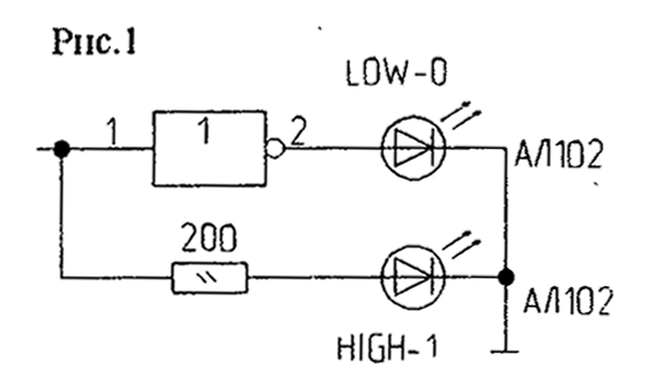
One of the options for the simplest probes is shown in Figure No. 1.
 Figure 1 – circuit diagram of a simple logic probe
 R1, R2 – 4.7 KOhm
VT1, VT2 – 2N2222
VD1 – green LED (any value)
VD2 – red LED (any value)
Operation and configuration of the digital probe circuit:
The circuit is powered by a 9 volt Krona battery. The principle of operation of the circuit is quite simple, transistors VT1, VT2 have n-p-n conductivity, so when you touch logical zero, the VD1 LED (green, or the color that you soldered in) lights up.
When you touch the logical one level with the probe, the transistor VT1 is unlocked and the LED VD2 lights up. If you get on the leg of a microcircuit that generates dynamic signals, both LEDs will light dimly. Instead of VD1 and VD2, you can solder a dual LED of the MV5491 type, which has two glow colors (with dynamic signals at the input, such an LED will light up amber). Adjustment of the probe’s operation is carried out by selecting resistors R1, R2 (it is more convenient to use trimming resistors instead).
5 / 13 041
Print version
For setting up and repairing ZX-Spectrum compatible computers, a useful device is a logic probe. Essentially, this is a device that displays the logical level of the signal at the input (log.0 or log.1). Since the logic levels may be different depending on the type of chip used (TTL, CMOS), the probe should ideally be configurable for use with different types of signals.ZX-Spectrums almost always use chips with TTL inputs/outputs, so it would be appropriate to consider the logic probe circuit taking into account TTL signal levels.
Here I will repeat a little the common truths, which are already known to everyone interested... The voltage values of log.1 and log.0 for TTL can be seen from the following schematic diagram:
As you can see, the extreme levels of log.0 and log.1 for inputs and outputs are somewhat different from each other. For the input, log.0 will be at a voltage of 0.8V or less. And the output level log.0 is 0.4V or less. For log.1 it will be 2.0V and 2.4V, respectively.
This is done so that the extreme levels of log.0 and log.1 for the outputs are guaranteed to fall within the voltage range for the inputs. That is why such a small “spread” was made in the levels of inputs and outputs.
Anything that falls within the voltage range between log.0 and log.1 (from 0.8V to 2.0V) is not recognized by the logic element as one of the logical levels. If there were no such difference in levels (2-0.8 = 1.2V), any interference would be regarded as a change in signal level. And so the logic element is resistant to interference with an amplitude of up to 1.2V, which, you see, is very good.
TTL inputs have an interesting feature: if the input is not connected anywhere, then the microcircuit “believes” that logic 1 is applied to it. Of course, such a “non-connection” is very bad, if only because in this case the input of the microcircuit hanging “in the air” “catches” all the interference, as a result of which false positives are possible. However, we are interested in something else - at the input “hanging in the air” there is always some voltage, the value of which falls in an indefinite interval between the logical levels:
There should be a video here, but it won't work unless you enable JavaScript for this site.
This level is called a “hanging unit”, i.e. as if there is a unit (it is regarded by the microcircuit as log.1), but in reality it is not there :)
In relation to the process of repairing and setting up computers, the concept of a “hanging unit” is useful in that if a conductor on the board breaks or the output of any microcircuit burns out, no signal is sent to the inputs of the microcircuits connected to them, and therefore there will be a “hanging unit”, and this moment can be recorded, because We already know the approximate voltage levels in this state of the microcircuit (on the order of 0.9V and up to 2.4V).
That is, if, for example, according to the circuit, the input of the microcircuit should be connected somewhere, but in reality it is not 0 or 1, but a “hanging one,” then something is wrong here. This is very useful in terms of the repair process!
Based on the above, we can formulate a technical specification for creating a logic probe:
- Voltage from 0 to 0.8V inclusive is considered as log.0;
- Voltage from 2.0V to 5.0V is considered as log.1;
- Voltages from 0.9V to 2.4V are considered as a “hanging unit”.
Various Logic Probe Designs
There are a lot of logic probe circuits. Just search in any search engine and enter the phrase “logical probe”. However, according to various criteria, these schemes do not suit me:- The output is sent to a seven-segment indicator, the brightness of which does not allow one to determine the approximate duty cycle of the pulses;
- There is no definition of a "hanging unit";
- Other criteria like “I just didn’t like the scheme” :)
A slightly more "advanced" version of this scheme:

I used this sampler for about 18 years. Despite its simplicity, this probe shows everything: log.0, log.1. It even shows a “hanging unit” - while the LED (log.1) barely glows. You can determine the duty cycle of pulses by the brightness of the LEDs. This probe does not even burn out when voltages of -5V, +12V and even higher are applied to its inputs! When -5V is applied to the probe, the LED (log.0) lights up with very high brightness. At +12V at the input, the LED (log.1) lights up with high brightness. In short, an indestructible scheme :)
To record short pulses that are not visible to the eye (for example, a port selection pulse), I attached a “latch” to the probe on the half of the TM2 trigger:

Probe appearance:

Your own version of a logic probe
I have attempted to make a logic probe with an indication of a “hanging one” on the comparators. In statics everything worked and was detected, but in dynamics the probe turned out to be inoperative. The problem lies in the speed of the comparators. The comparators available to me (LM339, K1401CA1, KR554CA3, etc.) are quite slow and do not allow operation at frequencies above 1.5-2 MHz. This is completely unsuitable for working with the ZX-Spectrum circuit. What's the use of a probe if it can't even show the processor clock speed?
But just recently on YouTube I came across a video lecture on the operation of a logic probe:
Lecture on the principles of operation of a logic probe
The lecture is very interesting and informative. Watch it in full!
This probe design interested me very much, and I decided to repeat it and test it. According to the diagram from the lecture, everything worked except for the cascade for determining the level of the “hanging” unit. However, this is not a problem, and I made a cascade on the comparator. There is no question of performance here, because... the term "dangling unit" applies to the static state of the chip.
The result was a probe with the following circuit:
P.S. The probe circuit is not the most ideal, and if desired, you can certainly make it simpler and better.
Description of the circuit and process of setting up a logic probe
The input stages of the probe are made on emitter followers on transistors VT1 and VT2. In the initial state (when nothing is supplied to the probe input), the transistors are closed, so logic 0 is applied to the inputs of DD1.1 through resistor R4, LED VD1 is not lit. In the same way, transistor VT2 is closed, and through resistor R5, logic 1 is supplied to the inputs of DD1.2, LED VD3 does not light up.When a signal with a level of log.0 (0...0.8V) is applied, transistor VT2 opens, log.0 is supplied to the inputs DD1.2, LED VD3 lights up.
When a signal with a level of log.1 (2...5V) is applied, transistor VT1 opens, log.1 is supplied to the inputs DD1.1, and LED VD1 lights up.
Resistors R2-R3 at the probe input set the voltage to about 0.87-0.9V. Those. It is necessary that this voltage be in the range of 0.8..0.9V so that the VD3 LED does not light up when the probe input is not connected anywhere.
A circuit for determining the “hanging unit” was made on the DA3 comparator. Resistors R6-R7 set a voltage of the order of 0.92..0.95V, at which the comparator will determine that the “hanging unit” level is at the input and the VD2 LED will light up. The voltage at the 2DA2 input is selected such a value that the VD2 LED does not light up when the probe input is not connected anywhere.
The color of the LEDs can be selected so that log.0 is shown in green, log.1 in red, and the “hanging unit” in yellow. I don’t know about you, but it’s more convenient for me. It is best to take transparent (not matte) LEDs VD1 and VD3, so that the crystal is clearly visible, and, if possible, bright, so that it is easier to replace if the LED glows even a little.
The DD3 chip contains a counter of pulses arriving at the input of the probe. With short pulses that are not visible to the eye, the VD4-VD7 LEDs will regularly show the number of pulses in binary form :) Using the SB1 button, the counter is reset with all LEDs going out.
The inverters of the DD2 chip are used to ensure that the active level (when the LED lights up) is log.0, because The TTL output at log.0 is capable of delivering current up to 16 mA to the load. With output logic 1, the output is capable of delivering a current of 1 mA, and if we connect an LED to it (so that it lights up with logic 1 at the output), we will overload the output. Current-limiting resistors are selected so that the maximum current flowing through the LEDs does not exceed 15 mA.
The probe is powered by a separate power supply (I used it from a Belarus tape recorder). Voltage stabilizer DA2 is located on the probe board. Considering that the current consumption of the probe is not too high, the stabilizer chip is used without an additional heat sink, and does not overheat.
The probe input circuits VT1, VT2, DA3 are powered by a separate reference voltage source DA1. This was done because when the current consumption of the probe changes (for example, when most of the LEDs are on), the output voltage of the DA2 stabilizer changes slightly, and all reference voltages will change accordingly, which is unacceptable.


